 |
DC
SQUID Magnetometer for characterizing the magnetic properties of bulk,
thin film, spin-glass, and super-paramagnetic nanoparticle systems.
± 5T DC fields can be applied to samples from 5K to 400K, with a
sensitivity of 1x10⁻⁷ EMU in the detected moment. |
 |
Vibrating sample magnetometer (VSM) for the rapid magnetic
characterization of materials. Optional cryostat and oven allow
temperature control from 5K to 1273K. Maximum field is ± 1.4T with a
moment sensitivity of 10-5 EMU. |
 |
X-ray
diffactometer (XRD) for the phase identification and structural
characterization of powder, thin-film, composite and nanoparticle systems.
Software is available for structural refinement and peak modeling for
strain and particle-size estimation. |
 |
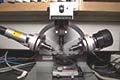
Scanning probe microscope (SPM) for the topological and structural
characterization of surfaces and the imaging of lithographed structures
and nanoparticle systems. By selecting the appropriate probes a
variety of techniques are available: contact and tapping atomic force
microscopy (AFM), lateral force microscopy (LFM) and magnetic force
microscopy (MFM). |
 |
X-ray
photoelectron spectroscopy (XPS) for the chemical characterization of
surfaces. The small inelastic mean free path of photoelectrons-- <
1nm-- makes this an exceedingly surface sensitive probe of element species
and chemical states. |
 |
Scanning electron microscopy (SEM) for the imaging of bulk, thin film,
patterned and nanoparticle systems. Energy analysis of the secondary
X-rays produced by the electron beam can be used to characterize the
elemental composition of the regions imaged. |
 |
e-beam
writing for nanolithography of devices. A focused electron beam is
used to expose special resists for patterning devices down to a length
scale of 30nm. This lithography tool is central to the fabrication
of nanoconstrictions, Hall gradiometers and spin-injection devices. |
 |
Photolithography for microlithography of devices. An ultraviolet
(UV) source is used to transfer the pattern of a mask onto a photoresist
covered surface. Subsequent development and etching produce a
structure in the shape of the mask. This lithography tool is used
for the fabrication of larger structures (e.g. Hall crosses for
magneto-transport measurements) and for the connections and contacts to
nanolithographed structures. |
 |
Focused
ion-beam lithography (FIB) uses a focused beam of gallium ions to directly
machine structures. This allows the fabrication of devices that can
not be fabricated using e-beam or photolithography due to complications
with wet or reactive ion etching. |
 |
Dip-pen
lithography uses a contact AFM tip to deliver chemicals directly to a
surface in controlled patterns. This lithography technique is
central to technologies that involve the self-assembly of nanostructures
from nanoparticles and nanotubes in solution. |
 |
Thermal
evaporation systems produce the gold, aluminum and lead thin-films
essential to the fabrication of self-assembled structures using dip-pen
lithography and tunneling junctions. |
 |
Molecular beam epitaxy (MBE) uses multiple shuttered effusion sources and
e-beam sources to form multilayers and superlattices of magnetic metals
and metal oxides. Electron diffraction (RHEED) allows for in situ
monitoring of film quality and thickness. |
 |
A
miniature e-beam evaporation system is devoted to the growth of EuS thin
films. EuS is a half-metal of great interest to spintronics
applications. |
 |
Reactive ion etching utilizes chemically reactive ions to etch
lithographed structures. This technique is a compliment to chemical
or "wet" etching. |
 |
Profilometry uses a stylus to scan across a sample profile its surface for
the purpose of estimating the size of patterned structures or measuring
film thickness. |
 |
Ellipsometry utilizes circularly polarized light to measure the thickness
of smooth films on substrates. This is a totally noncontact
technique for characterizing film thickness. |
| |
|
| |
|
| |
|
| |
|